Reverse-engineering ADAX WT2 thermostat
When I was in the market for some resistive heaters, I wanted to get some with a local API. ADAX had just started offering heaters with the WT2 WiFi and Bluetooth thermostat. For those, a local API had been documented at the time. The API is somewhat quirky and the devices don't always behave stable, so curiosity got the better of me and I had to have a look inside.
Hardware

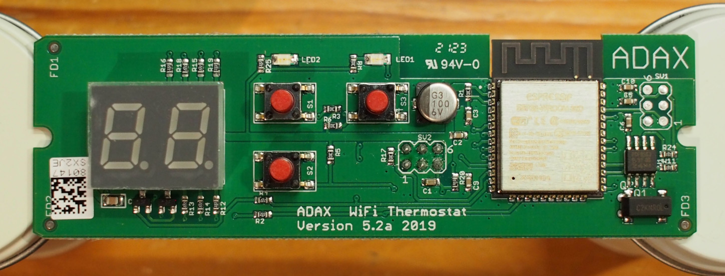
Somewhat unsurprisingly, the operation is run by an ESP32 SoC that comes in the form of the ESP32-WROOM-32D module. I'm guessing that the previous generation of the thermostat that lacked BLE has been equipped with an ESP8266. The SV2 pinheader connects to the high-power part of the heater. U1 is a PCF8563 real-time clock.

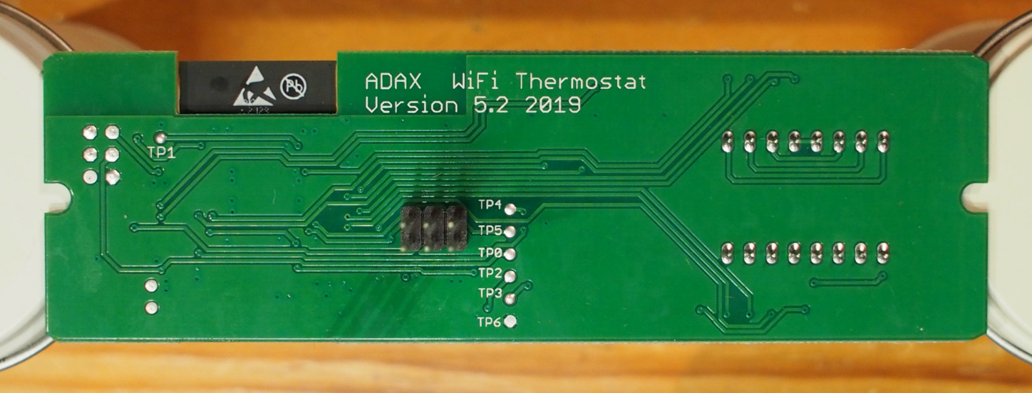
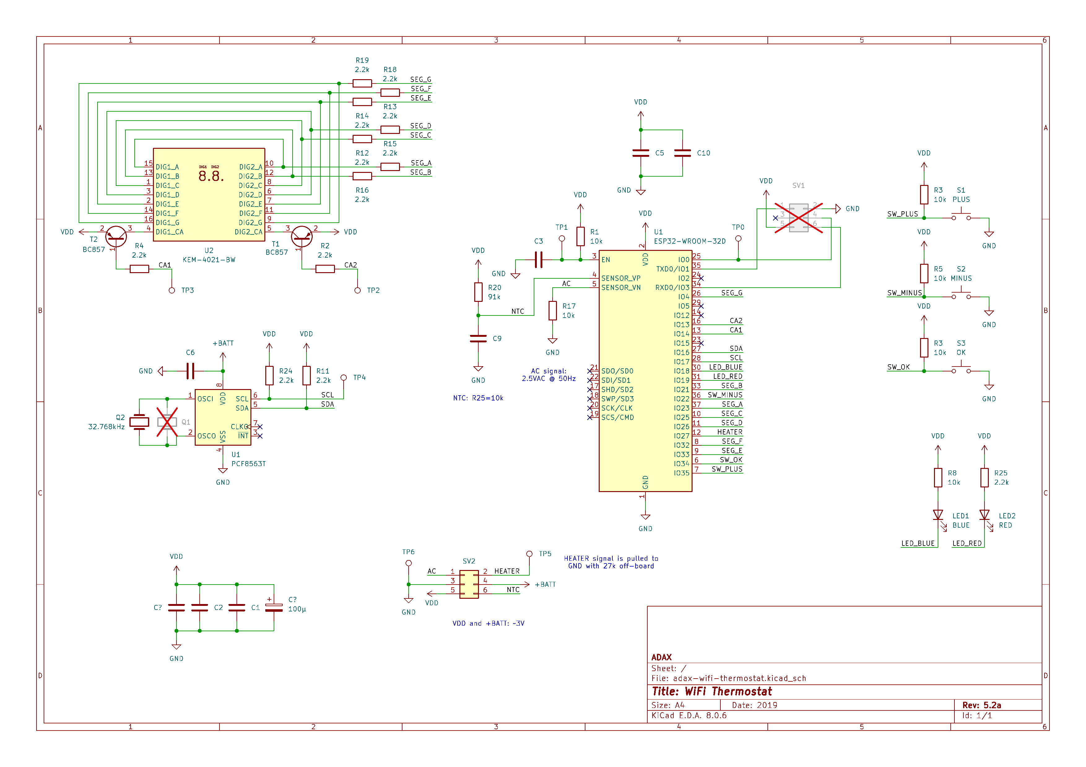
Mostly as an exercise, I decided to reverse-engineer the schematics. I did this by overlaying a picture of the frontside of the PCB with a mirrored picture of the backside of the PCB and then play with the opacity of the backside layer as I go along. I added some annotations where necessary.

Using this method I was able to draw the complete schematics. Since some traces are hidden under the ESP32 module, I used a multimeter in continuity mode in addition.

I would say there are no real surprises here. However, the unpopulated UART
and programming header SV1 immediately made me wonder whether the ESP32 would
be fused to prevent reading out of the flash memory. So I sucked/wicked the
solder out of the holes and soldered in a pinheader in order to be able to
hook up an FT232H. I powered the board with IO0 tied to ground
which brings the ESP32 into serial bootloader mode and then launched
esptool.py with --before no_reset which promptly
detected the ESP32-D0WD (revision v1.0) and 8MB of flash which I was able to
read out without issue — nice!
Firmware
Using esp32_image_parser with a small modification I was able to extract the following partition table:
| Label | Offset | Length | Type | Sub type |
|---|---|---|---|---|
| nvs | 0x009000 | 0x004000 | 1 [DATA] | 2 [WIFI] |
| otadata | 0x00d000 | 0x002000 | 1 [DATA] | 0 [OTA] |
| phy_init | 0x00f000 | 0x001000 | 1 [DATA] | 1 [RF] |
| ota_1 | 0x010000 | 0x150000 | 0 [APP] | 17 [ota_1] |
| spiffs | 0x160000 | 0x0f0000 | 1 [DATA] | 130 [spiffs] |
| ota_0 | 0x250000 | 0x150000 | 0 [APP] | 16 [ota_0] |
0x8000While the ota_0 partition was empty, the ota_1
partition contained the firmware. Briefly grep-ing for strings in the firmware
blob reveiled that we're looking at firmware version 2.0.1.8. I was interested
in the control aspects of the firmware should I ever attempt to replace the it
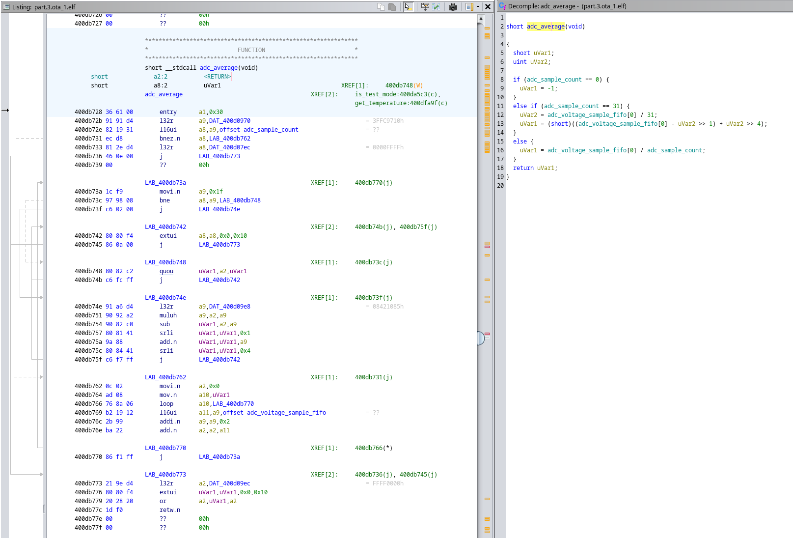
with my own implementation. So I set out to open this code in Ghidra.
James Warner has a pretty good
write-up on
the topic. The SVD load script threw a few errors so not all peripheral
registers got populated but that wasn't a big deal. What was a bit confusing
was Ghidra failing to detect loops in certain locations.

I found the function that calculates the temperature from the ADC input
voltage at 0x400db4fc:
int points[] = {
  54820, 51940, 49230, 46680, 44280, 42010, 39870, 37860, 35950, 34160,
  32460, 30860, 29340, 27910, 26560, 25280, 24060, 22920, 21830, 20810,
  19830, 18910, 18040, 17210, 16420, 15680, 14970, 14300, 13660, 13050,
  12480, 11930, 11410, 10920, 10450, 10000,  9574,  9169,  8784,  8416,
  8066,   7733,  7415,  7112,  6823,  6547,  6284,  6033,  5793,  5564,
  5345,   5136,  4936,  4746,  4563,  4388,  4221,  4062,  3909,  3762,
};

// returns temperature in hundreds of degrees centigrade
int calc_temperature(unsigned short adc_mv)
{
  int r_ntc;
  float r_ntc_float = (float)adc_mv / (3000.0f - (float)adc_mv) * 91000.0f;
  if (r_ntc_float <= 0.0f)
    r_ntc = 0;
  else
  {
    if (r_ntc_float != r_ntc_float) // NaN
    {
      r_ntc = -0x80000000;
      if (r_ntc_float >= 0.0f)
        r_ntc = 0x7fffffff;
    }
    else
      r_ntc = (int)r_ntc_float;

    if (r_ntc >= points[0])
      return -1000;
  }

  for (int i = 0; i < ARRAY_LENGTH(points) - 1; ++i)
  {
    if (r_ntc > points[i + 1])
      return ((r_ntc - points[i]) * 100) / (points[i + 1] - points[i]) + (i + 1) * 100 - 1100;
  }
  return 4900;
}
The ADC input voltage plotted against the calculated temperature yields the following graph:
calc_temperature() input vs. outputFrom this (current) temperature and a set target temperature, the heater duty
cycle is calculated. The period is fixed to 120 s. The 0x400dfb30, this is the relevant excerpt:
int calc_heat_time(int temperature, int target)
{
  int heat_time = 0;
  if ((temperature_valid != false) && target > 0)
  {
    heat_time = 120;
    int delta = ((target + 50) - temperature) - temp_offset;
    if (delta <= 400)
    {
      heat_time = 0;
      if (delta > 0)
      {
        heat_time = (delta * 9000) / 25000;
        if (heat_time > 90)
          heat_time = 90;
      }
    }
  }
  return heat_time;
}
calc_heat_time() input vs. outputThere is a lot more to discover in the firmware, e.g. there is a local API
endpoint /api?command=info which yields device an firmware
information and it is not documented. One thing that bugged me a bit was that
I didn't find the code that enables and disabled the red LED that indicates
that the heater is on. I couldn't find any trace of the SENSOR_VN
pad being used — either as a digital I/O pin or an ADC input. I'm guessing,
its original purpose was zero-crossing detection.